MAG*I*CAL traceable TEM calibration standard
An accurately calibrated TEM is imperative for generating correct imaging data. Using a traceable MAG*I*CAL calibration standard, allows your TEM can be accurately calibrated. The MAG*I*CAL traceable TEM calibration standard consists of four sets of five SiGe layers with a thickness of ~10nm, alternating with pure silicon layers with a thickness of ~13nm. The total thickness of the set of alternating layers is ~100nm. The distance between each set of five layers is ~1.2µm. The epitaxial layers are grown using an MBE (Molecular Beam Epitaxy) process on a single crystal silicon {001} substrate.
The finished calibration standard is a cross-sectioned TEM calibration sample with four regions where the calibration lines can be imaged.
Left: Optical image of the four regions of the calibration structures
Middle: Diagram of the four regions of the calibration structures
Right: TEM image of four identical structures with alternative Si/Si Ge lines


Left: Lattice image of the Si single crystal
Middle: Kikuchi pattern from the Si single crystal for alignment
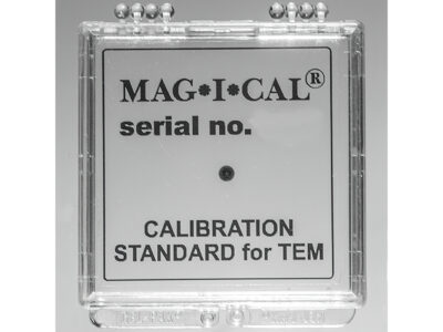
Right: MAG*I*CAL is delivered in a convenient gel box


MAG*I*CAL TEM magnification calibration standard can be used to calibrate:
- The TEM over the entire range from 1000x up to 1,000,000x magnification with the alternating lines
- Camera-constant calibration using the Si single crystal
- Image / diffraction pattern rotation calibration using the Si single crystal area
The four sets of alternating layers of Si and SiGe provide light and dark lines with good contrast. The four sets are calibrated using a high-resolution transmission electron microscope (HR-TEM) with reference to the {111} lattice space of silicon (0.3135428nm) measured on the single crystal substrate of a MAG*I*CAL calibration standard. This method provides unbroken traceability of a fundamental constant of nature, the lattice constant of silicon.
Each MAG*I*CAL calibration reference standard is supplied mounted within a 3mm titanium disc. A calibration manual is included.
Traceability of the MAG*I*CAL TEM calibration reference standard
The MAG*I*CAL calibration reference standard is manufactured from a single crystal silicon wafer, and so incorporates a fundamental constant of nature into the standard – the crystal lattice constant of silicon. All calibration markings on the standard are directly referenced to this natural constant. The calibrated values can be verified by the user by observing the crystal lattice image of the silicon substrate and validating the calibrated values.
Natural Metrology Institutes (NMI’s) such as NIST in the USA, NPL in the UK and PTB in Germany, etc., certify measurements as traceable to fundamental constants of nature, but they do not certify natural constants. The MAG*I*CAL calibration reference standard does not require NMI certification since the calibration is directly traceable to a natural constant available on the standard itself (the crystal lattice spacing of silicon) and all calibrated values can be verified by the user. The crystal lattice spacing is an intrinsic property of a material. For pure silicon, the crystal lattice spacing has been well characterised and documented by the scientific community. It is known to be better than eight decimal places: 0.313560136 nm. This value can be obtained from a recent CRC Handbook of Chemistry and Physics and many other references.