Welcome to Labtech-EM, if you can’t find what you’re looking for please get in touch via our contact us page.
Product Quick Find
Welcome to Labtech-EM
We have an extensive range of innovative, market-leading accessories, consumables and instruments for electron microscopy. We pride ourselves on our fast and friendly service, supported by a team with an extensive background in electron microscopy preparation. We look forward to hearing from you and being of service…
TEM and cryo TEM products
Grids, Diatome knives, stains, carbon coaters, plasma cleaners, TEM stains and more…
SEM & FIB products
Adhesives, stubs, stub boxes, filaments, sputter/carbon coaters, adaptors and more…
LM & AFM products
Substrates, calibration, cleaning, storage, small tools and general specimen preparation etc…
Featured Products
-
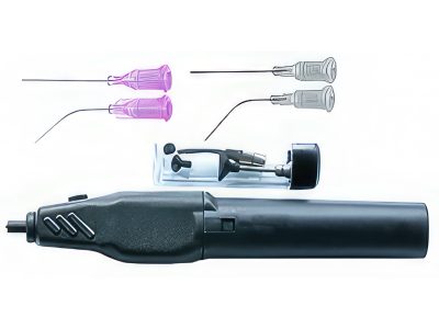
Micro-Tec B126 ESD safe battery operated vacuum pen
Micro-Tec B126 ESD safe battery operated vacuum pen with two tips, three vacuum cups and fine needles for TEM grid handling.
£47.83 Add to basket -
vacuum sample storage container for 19 x Ø12.7mm pin stubs
EM-Storr 81P vacuum sample storage container for 19 x diameter 12.7mm pin stubs (each)
£390.56 Add to basket -
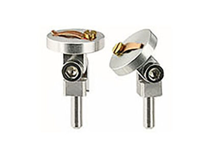
PS15C pin stub swivel mount sample holder with one S-Clip – pin
EM-Tec PS15C Pin stub swivel mount sample holder with 1 x S-Clip – pin (each)
£42.57 Add to basket -
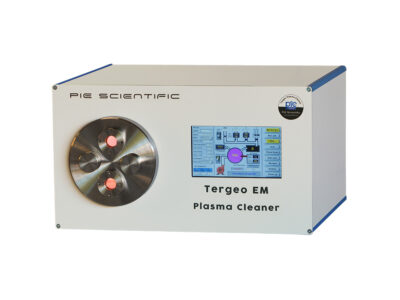
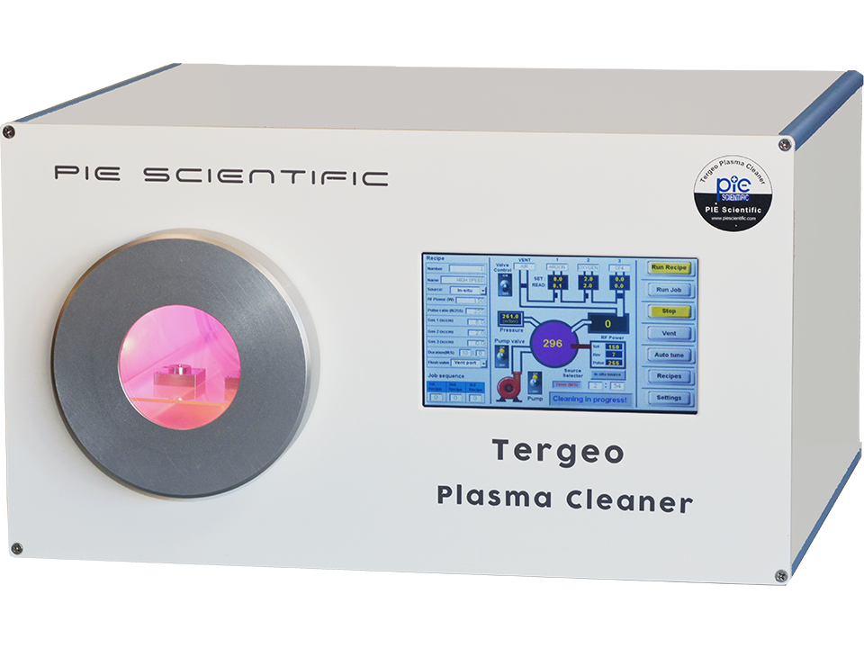
Tergeo-EM tabletop plasma cleaner
Tergeo-EM tabletop plasma cleaner with Direct/immersion and downstream/remote plasma sources in one system. Plasma emission sensor for quantitative plasma emission intensity measurement.
Price On Request Read more
75W 13.56MHz high frequency RF supply.
EM product and event news
New – gold coated slides and coverslips
Designed for microscopy, AFM /SPM, nanotechnology and biotechnology applications. They can also be used as opaque light microscopy supports or gold coated substrates in a range of experiments. Slides and coverslips are pre-cleaned before coating and coated with gold...
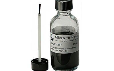
New – C30F water-based carbon paint
EM-Tec C30F is a water-based conductive carbon paint with finely dispersed graphite flakes (~<1 - 2μm, maximum 5um). It does not contain any hydrocarbon-based solvents and is fully compatible with high vacuum systems - and even UHV applications when dry. For...
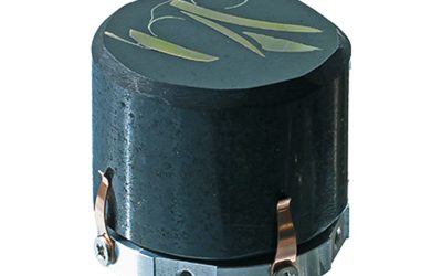
New – compact Smart-Clip metallographic mount holders for SEM
Specifically designed for compact and table-top SEMs and for high-tilt applications. They have a low weight, minimal diameter and allow for very high tilt angles – close to 90 degrees. For details and pricing see; Smart-Clip metallographic mount holders