Silicon SEM finder grid substrate
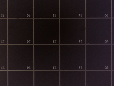
EM-Tec FG1 silicon SEM finder grid substrate consists of a 12 x 12mm chrome-deposited grid with a 1mm pitch on a conductive ultra-flat silicon substrate. The substrate is divided into 144 indexed fields of 1 x 1mm, where each of the fields has a unique alphanumeric label in the lower right corner. The alphanumeric label is easy to see with a magnifier, stereo microscope and/or SEM. The grid produced is comparable with 25 mesh and is practical for larger particles or small specimens mounted on the substrate in separate fields.
The EM-Tec FG1 silicon SEM finder grid substrate is ideal for correlative microscopy since the position of the specimen is easily located. Size of the EM-Tec FG1 is 12 x 12mm on a 12.5 x 12.5mm substrate. Primarily designed for SEM applications, but equally suitable for reflected light microscopy, AFM and Auger/SIMS.
EM-Tec FG1 finder grid is ideal for:
- Correlative, corroborative, collaborative and repetitive microscopy
- Multi-specimen mounting for small specimens
- Demonstration specimens with quick finder grid
- Quick size estimation with the 1mm grid

Details of pattern and ultra-flat silicon wafer
| Pattern size | 12 x 12 mm divided into 144 individual 1 x 1mm fields |
| Numbering | Each field has unique alphanumeric label in lower right corner |
| Pattern/labels | 75nm thick deposited Cr with 20µm line width, 80µm label height |
| Substrate size | 12.5 x 12.5mm |
| Orientation | <100> |
| Type | P (Boron) |
| Resistance | 1-10 Ohm/cm |
| Grade | Prime/CZ Virgin |
| Coating | None, native oxide only |
| Thickness | 675µm (+/- 20µm) |
| TTV | ≤1.5µm |
| Warp | ≤30µm |
")